

 English
  Tiếng Việt
 ELECTRONIC NEWS HIGHLIGHT W24.2025
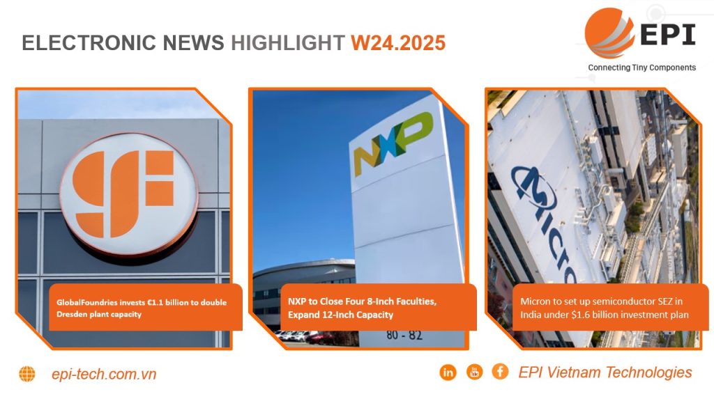
1. GlobalFoundries invests €1.1 billion to double Dresden plant capacity
GlobalFoundries (GF) has announced plans to invest €1.1 billion over the coming years to double wafer production capacity at its Dresden, Germany, facility to 1.5 million wafers per year. The facility specializes in 22nm FD-SOI 22FDX low-power process technology for power and RF devices and supports 28nm, 40nm and 55nm nodes primarily targeting automotive and IoT microcontrollers.
The Dresden site currently operates 60,000 square meters of cleanroom space and employs approximately 3,200 people. The expansion is benefiting from significant financial support from the German government, including hundreds of millions of euros, and GF is pursuing an additional €1 billion in funding under the EU’s Important Projects of Common European Interest (IPCEI), which will be approved in June 2023.
On the technology front, GF has a strategic partnership with Indie Semiconductor to develop 77GHz and 120GHz radar SoCs based on the 22FDX process for advanced driver assistance systems (ADAS). GF is also collaborating with Bosch on a single-chip radar sensor using the same process and with Ayar Labs to develop the industry’s first UCIe optical interconnect chip leveraging a monolithic photonic platform.
In the midst of competition, the German government is also providing €1 billion in funding for Infineon’s smart power plant in Dresden. Meanwhile, TSMC is partnering with NXP and Bosch to build the ESMC wafer fab in Dresden, focusing on 28nm and 22nm technology, backed by a €5 billion European subsidy.
GF previously announced an additional $3 billion investment in its US fabs in Malta, New York and Vermont, including CMOS manufacturing, gallium nitride (GaN) manufacturing and a new advanced packaging and photonics centre, although US government support for the fab and Vermont packaging centre is being scaled back.
Learn more: GlobalFoundries invests €1.1 billion to double Dresden plant capacity
2. NXP to Close Four 8-Inch Faculties, Expand 12-Inch Capacity
NXP Semiconductors will shut down four 8-inch wafer fabs—one in Nijmegen, the Netherlands, and three in the United States—over the next decade as it shifts production to more efficient 12-inch fabs.
The move is driven by the economics of 12-inch wafers, which offer about 2.25 times more power per wafer than 8-inch wafers, resulting in significantly lower fixed and manufacturing costs. This is in line with the broader industry trend toward larger wafer sizes amid surging demand for AI and data centers.
In a strategic expansion, NXP plans to leverage its joint venture with Vanguard International Semiconductor (VSMC) in Singapore, targeting 12-inch volume production by 2027 and a monthly production target of 55,000 wafers in mixed-signal and analog chips by 2029. The facility will serve as a manufacturing hub for the Asia-Pacific region.
Industry data shows that global 12-inch wafer capacity is expected to reach 9.6 million wafers per month by 2026, accounting for about 65% of silicon substrate sales, while 8-inch wafer capacity accounts for only about 20%.
Analysts say NXP’s fab consolidation is driven by the combined pressures of market demand, manufacturing efficiency, and competitive cost structures. While scaling to 12-inch fabs requires significant investment and complex processes, NXP’s foundry and partnership strategy allows the company to balance advanced node capabilities with mature process volumes. Maintaining optimal cost and geographic distribution will be critical to the company’s success.
Learn more: NXP to Close Four 8-Inch Faculties, Expand 12-Inch Capacity
3. Micron to set up semiconductor SEZ in India under $1.6 billion investment plan
Micron Technology has received approval from the Indian government to set up a semiconductor-focused special economic zone (SEZ) in Sanand, Gujarat, under a planned investment of 130 billion rupees (about $1.6 billion). The SEZ, spread over 37.64 hectares, will support advanced chip assembly, testing and packaging operations, bolstering India’s domestic semiconductor manufacturing capabilities.
The move is part of India’s broader strategy to attract global semiconductor companies and localize high-tech manufacturing. In parallel, Hubballi Durable Goods Cluster Private of Aequs Group has also received approval to set up a Rs 1 billion SEZ for electronic components in Dharwad, Karnataka.
These developments follow new SEZ regulations introduced on June 3, which ease land and regulatory requirements for semiconductor projects. The reforms lowered the minimum land threshold for electronics SEZs from 50 hectares to 10 hectares, allowed domestic supply after payment of taxes, and eased mortgage and ownership conditions. Additionally, the changes allow free goods to be included in net foreign exchange (NFE) calculations, using customs valuation standards.
The revised regulations are aimed at building a robust semiconductor manufacturing ecosystem, attracting targeted investment and creating high-skilled jobs, the Indian commerce ministry said. Micron’s project is seen as a milestone in India’s efforts to become a key player in the global chip supply chain.
Learn more: Micron to set up semiconductor SEZ in India under $1.6 billion investment plan
#ASEAN #AsiaPacific #distributor #Global #electronicdistributor #PCBA


Related News
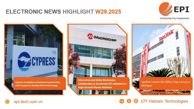
ELECTRONIC NEWS HIGHLIGHT W29.2025
1. Cypress strengthens photomask partnership with Toppan to develop 65nm technology Cypress Semiconductor Corp. has expanded its partnership with Toppan Photomasks Inc. through a new joint development agreement focused on 65-nanometer photomask technology, along with an extended multi-year supply agreement. Under the three-year agreement, Toppan’s facility in Round Rock, Texas, will provide the majority of […]
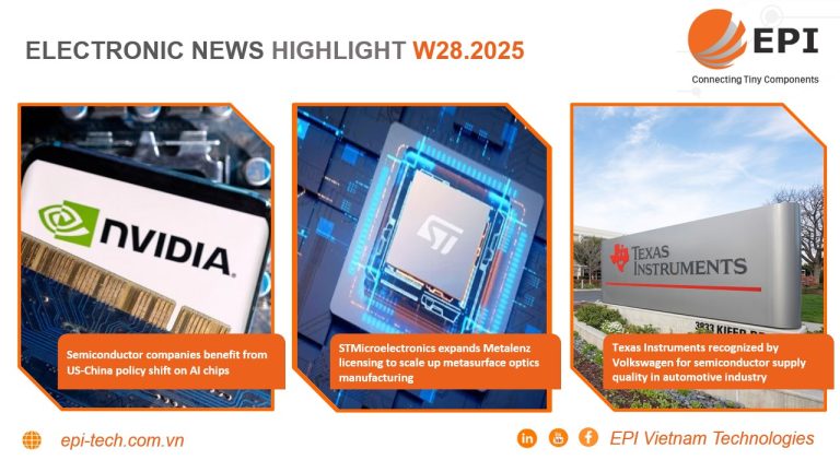
ELECTRONICS NEW HIGHLIGHT W28.2025
1. Semiconductor companies benefit from shifting US-China policy on AI Chips The adjustment in the United States’ policy on AI chip exports is beginning to ease trade tensions with China, prompting reactions from major semiconductor companies including Nvidia, AMD, and Apple. On July 14, 2025, Nvidia announced that it had submitted a request to the […]
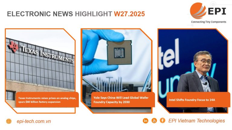
ELECTRONIC NEWS HIGHLIGHT W27.2025
1. Texas Instruments raises analog chip prices, fueling $60 billion factory expansion Texas Instruments is increasing prices on a range of data converter and analog chips, with some devices seeing price hikes of up to 100%, according to analysts at Bernstein. The move is aimed at boosting profit margins rather than responding to any […]
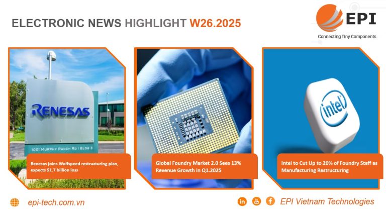
ELECTRONIC NEWS HIGHLIGHT W26.2025
1. Renesas joins Wolfspeed restructuring plan, expects $1.7 billion loss Renesas Electronics said it has signed a Restructuring Support Agreement (RSA) with Wolfspeed and the company’s major creditors, as Wolfspeed prepares for a court-supervised restructuring under Chapter 11 of the U.S. Bankruptcy Code. Renesas could record an impairment loss of up to 250 billion yen […]